Our universal approach enables our systems to perform a large variety of processes. The reactor unit is customizable in a simple a quick way, which allows short lead times for highly customized systems.
A selection of processes available in our systems:
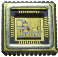
die-attach – One of the most common applications using vacuum solder reflow systems. Usually, bare dies as e.g. IGBT, power or laser diodes, MEMS etc. are placed on a substrate, leadframe or another semiconductor package. A metal preform or printed solder paste is used to form a permanent joint during the reflow process. The perfect process maintaining an optimal combination of materials, process parameters and equipment means voidless joint, stable height of bonding pads, and no critical die shift.
Substrate soldering – The large area soldering of DBC and AMB substrates is a very demanding process for the vacuum solder reflow system. Especially in power modules manufacturing, beside void free joints and absence of shrinkage cavities, the performance of the soldering system has to ensure high throughput, low cost of ownership and robustness in a mass production environment. For soldering of double-sided cooling modules, it needs a high level of flexibility for implementation of various fixtures to keep geometrical dimensions in a small tolerance window.
Package sealing – To ensure the protection of electronic devices against environmental conditions they are commonly sealed in a ceramic or metallic package, which provides a mechanical support and electrical feedthroughs. In some applications as e.g., packaging of microbolometers and gyroscopes the device has to be encapsulated in vacuum. The requirements on a vacuum reflow system include the control of the outgassing from packages and devices as well as the chamber atmosphere. This is essential for a solder joint with ultra-low leak level.
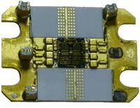
T/R modules – Highly reliable solder joints are crucial in manufacturing of high frequency devices in variety of space, airborne and ground applications. Fluxless processes using formic acid or hydrogen as reducing agent are well established.
Wafer bump reflow – Solder and pillar bumps of many different materials are used in flip chip and wafer level soldering. They can be screen printed using solder paste, electrochemically deposited or placed on the wafer via solder sphere transfer process. In a following solder reflow process bumps are shaped to a uniform geometry and joined to the under-bump metallisation. Depending on the bump fabrication method the reflow process can be with flux or fluxless. In a fluxless reflow the cleaning process is done in the reflow chamber using e.g., plasma or formic acid depending on the material composition of the bumps.
Wafer level packaging (WLP) enables on the one hand the extreme miniaturisation of the package form factor and reduction of the costs per device. On the other hand, it makes new approaches in 3D packaging and heterogeneous integration possible crucially improving the device performance.
Brazing - Using high temperature melting point solders based on silver or glass can be used to join parts made of stainless steel, kovar®, ceramics etc.
Further thermal processes as annealing, sintering and alloying on substrate or wafer level can be applied to change the material composition, chemical and physical properties. Beside an excellent temperature control during the entire profile, they require very good temperature uniformity and repeatability.
Haven't found your process? Do not hesitate to contact us to give us a chance to make your process happen in our system. With your samples we can test feasibility and quality of your process in our system.